Ads
Nanoscale quakes slash memory chip power by one billion times
4 ngày trước
00NANOSCALE QUAKES SLASH MEMORY CHIP POWER BY ONE BILLION TIMES
Imagine building a colossal toy tower out of thousands of interlocking plastic bricks. To dismantle it and pack it into a box, you would simply nudge the base and let the rows tumble into an untidy pile on the floor. Yet for decades, the most advanced phase-change memory chips have accomplished this task through brute force: blasting memory cells with electric pulses past eight hundred degrees Celsius to melt the crystal lattice, then freezing it instantly into disordered glass. This melt-quench cycle burns immense amounts of electricity and rapidly degrades electronic components.
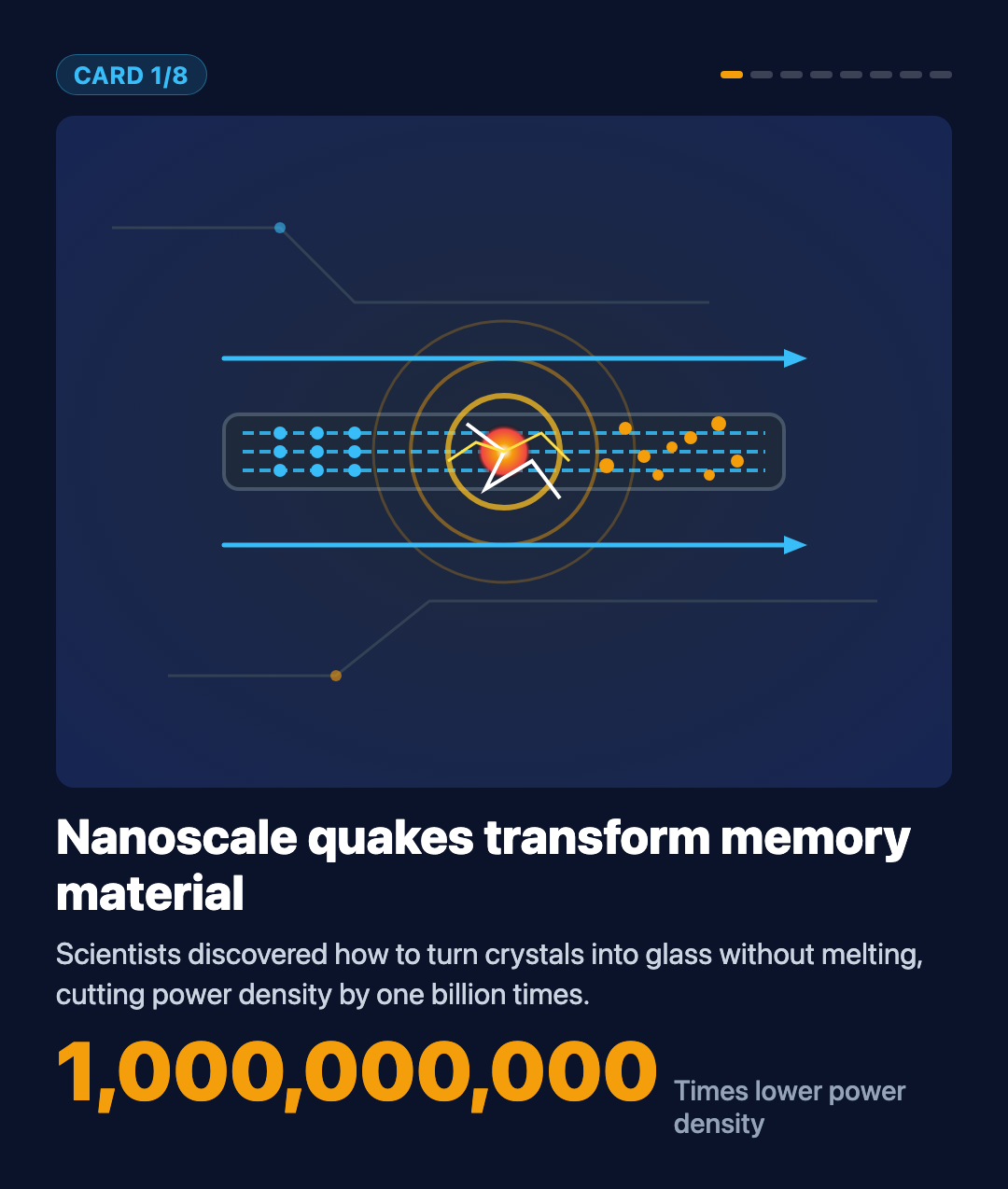
On November 13, 2026, in the scientific journal Nature, an international research team led by the University of Pennsylvania, the Indian Institute of Science, and the Massachusetts Institute of Technology announced a game-changing breakthrough: they discovered how to transform memory materials from crystal to glass entirely in the solid state without heating, slashing switching power density by one billion times.
WHAT WAS THE ORIGINAL PROBLEM?
In the digital realm, every photograph, song, and artificial intelligence calculation boils down to binary zeros and ones. To record these bits at lightning speed, engineers developed phase-change memory. Its core concept mimics a structural puzzle: when atoms are neatly aligned like transparent crystal lattices, electric current flows with little resistance, representing a binary zero. Conversely, when atoms are jumbled like grains in opaque glass, resistance surges, registering a binary one.
Phase-change memory promises speeds thousands of times faster than conventional flash drives, but thermal demands have shackled its widespread adoption for fifty years. Resetting a bit required superheating the cell past eight hundred degrees Celsius before quenching it. This relentless thermal cycling demands excessive electrical power, generates massive heat, and eventually cracks delicate microcircuitry.
Note – Phase-change memory: A data storage device that records binary information by toggling material between an orderly crystal state and a disordered glass state.
WHAT CHANGED COMPARED TO PREVIOUS BELIEFS?
For generations, condensed matter physics textbooks taught that transforming an ordered crystal lattice into an amorphous glassy network inevitably required melting through a liquid phase followed by rapid quenching. Experts assumed it was fundamentally impossible to scramble millions of atoms across long distances while keeping the material completely solid and cool.
The new study overturns that longstanding assumption. By examining a fragile two-dimensional layered semiconductor, the researchers demonstrated that solid-state amorphization can be triggered electrically at room temperature. Rather than relying on heat, an ordinary electric field sets off subatomic collisions that propagate like miniature earthquakes. This cascade creates an avalanche effect that topples the crystal lattice without liquefying a single atom.
Note – Solid-state amorphization: The structural transformation of an orderly crystal directly into disordered glass within the solid state, without heating into liquid.
Note – Avalanche effect: A cascading chain reaction where a small initial perturbation triggers collisions that multiply rapidly, much like a rolling pebble unleashing an avalanche.
HOW DID SCIENTISTS DISCOVER THIS?
The secret to this achievement lies in indium selenide, an exotic two-dimensional semiconductor composed of stacked atomic sheets loosely bound like pages in a notepad. When the team applied an electric field across indium selenide nanowires, traveling electrons exerted a mechanical drag known as carrier wind force. This force nudged the atomic sheets, causing them to slide against one another.
As the crystal planes slid and collided against internal domain boundaries, they generated localized, self-induced shockwaves. These nanoscale earthquakes cascaded through the material, knocking the ordered crystal lattice into an amorphous glassy state in an instant. To capture this transformation, researchers utilized in-situ transmission electron microscopy, observing the sliding atomic layers and measuring structural transitions in real time. Quantitative measurements confirmed that the required power density plummeted by a factor of one billion compared to standard melt-quench methods.
Note – Indium selenide: A layered semiconductor made of atomically thin two-dimensional sheets that slide against each other when stimulated by an electric field.
Note – Carrier wind force: A directional mechanical force exerted by flowing electrical charge carriers onto atoms in a crystal lattice, similar to wind blowing paper sheets.
Note – In-situ transmission electron microscopy: An advanced electron microscope that beams electrons through specimens to record atomic-scale structural changes during real-time electrical stimulation.
WHAT DOES THIS MEAN FOR HUMANITY?
This discovery opens unprecedented possibilities for the global semiconductor industry. With artificial intelligence data centers consuming national-scale power grids, memory chips that operate on one-billionth the power density could drastically alleviate planetary energy strains and carbon footprints.
Beneficiaries range from high-performance supercomputing facilities to everyday mobile devices. Ultra-low-power solid-state phase-change memory could allow smartphones to expand memory capacity while running for days on a single charge, while server farms could shed billion-dollar cooling infrastructures.
Nevertheless, moving from laboratory discovery to commercial silicon wafers remains a multi-year endeavor. The findings represent basic research conducted on isolated nanowires. Scientists must still determine whether the material can endure billions of read-write cycles without degradation. Furthermore, integrating indium selenide into standard industrial silicon foundry processes presents significant fabrication hurdles.
The research team plans to build multi-element memory arrays, evaluate endurance over extended cycles, and test similar avalanche amorphization in other layered materials. If successful, this cold atomic earthquake could serve as the cornerstone for green computing in the artificial intelligence era.
SOURCES
Nature – Electrically driven long-range solid-state amorphization in ferroic In2Se3 – https://doi.org/10.1038/s41586-026-11252-8
University of Pennsylvania – Researchers achieve solid-state amorphization in 2D ferroelectric memory – https://penntoday.upenn.edu/news/solid-state-amorphization-ferroelectric-memory-2026
Indian Institute of Science – Breakthrough in ultra-low-power phase-change data storage – https://iisc.ac.in/news/2026/11/solid-state-amorphization-in2se3
0 comments
Ads
Related Posts
Ads